Solutions
Published
16 December 2025
Written by Yunus Unal Mechatronics Engineer and Content Specialist
Yunus is a mechatronics engineer with a background in 5G mobile communications and intelligent embedded systems. Before joining TKO and ipXchange, he developed and tested IoT and control-system prototypes that combined hardware design with embedded software. At ipXchange, Yunus applies his engineering knowledge and creative approach to produce technical content and product evaluations.
Low current coin cell systems demand aggressive power saving at every level. The goal is to minimize standby current and only wake the CPU when strictly necessary. In practice, this means using deep sleep modes, ultra low quiescent current (Iq) components, and smart firmware/peripheral designs. This article surveys techniques duty cycling, DMA offload, sensor fusion and low Iq hardware that embedded engineers can apply to maximize coin cell battery life. We emphasize concrete examples and leading 2025 platforms (STM32U0, NXP MCX-L, TI MSPM0, Renesas RA0/RA4, SiLabs EFR32, Nordic nRF54) throughout.
Coin cells have limited capacity and discharge down to around 3V. A typical CR2032 might last years only if the average current is in single digit microamps. In practice, even 10 year lifetimes are elusive, so designs target around 5-10 µA average. Thus, standby current reduction is paramount. All design choices, from MCU selection to pull‑ups on I/O’s, must favour minimal leakage and quiescent draw to extend coin cell battery life.
Duty Cycling and Sleep Modes for Coin Cell Battery Life
The cornerstone technique is duty cycling is keep the MCU and sensors asleep as much as possible, waking briefly for tasks. Modern low power MCUs offer deep sleep or standby modes with nA-µA draw. For example, STM32U0’s STOP2 mode with full RAM retention draws only ~630 nA, and a special “Standby” mode is just 30 nA (with only 6 pins active).
In firmware, use the Wait For Interrupt (WFI) or Wait For Event (WFE) instruction to enter sleep. Configure a real time clock or low power timer as the periodic wake source. Prioritise wakeups carefully, enable only the interrupts needed and keep others masked. Disable or gate off peripherals when idle. Enter the lowest-power mode that meets latency requirements. Stop or halt the CPU clock with WFI/WFE; disable PLLs, USB, LCD, etc. For instance, many STM32s and nRF chips have “System OFF” or “Shutdown” modes yielding ≪1 µA draw. When awake, do as much work as possible in one burst, then go back to sleep. Batch sensor reads and communication rather than waking frequently. Use low-speed clocks (32 kHz crystal) or asynchronous wake units. If multiple interrupts exist, use priority settings so the most energy-critical sources wake the device. Tie unused GPIOs to safe states (no floating pins). Turn off high-frequency oscillators; many MCUs can wake from a low-speed crystal and then enable a fast clock when needed.
By aggressively using stop/shutdown modes and minimizing CPU on time, designers can cut the average current dramatically. This duty cycling forms the first line of defence for extending coin cell battery life.
DMA and Autonomous Peripherals for CPU Offload
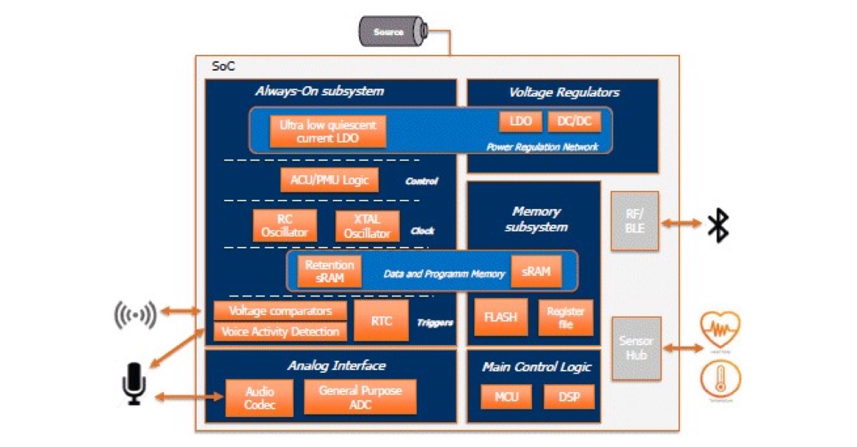
Beyond basic sleeping, we can offload work from the CPU altogether. Direct Memory Access (DMA) peripherals allow data transfers (SPI, I²C, ADC reads, UART, etc.) without waking the CPU, so the core stays in WFI/WFE. For instance, many MCUs include multi-channel DMA controllers (e.g. NXP’s LPC55S66 has two DMA units with 22 and 10 channels). This lets the MCU set up a sensor or ADC to fill a buffer via DMA, then sleep until an interrupt signals the buffer is ready. Without DMA, the CPU would have to wake for every byte or sample.
Figure: Example ultra-low-power MCU block diagram (NXP LPC55S66) showing dual Cortex-M33 cores, multiple DMA controllers (22ch, 10ch), low-power timers/oscillators, and peripherals. Such integrated DMA channels allow data transfers (e.g. from sensors) to happen autonomously while the CPU sleeps.
Key firmware tips:
- Configure DMA for Sensors: Have the ADC, SPI, or I²C peripheral use DMA to move samples into RAM. The CPU can sleep or do other tasks; only wake on “buffer full” interrupt.
- Peripheral Autonomous Modes: Use sensors’ built-in features. Many MEMS sensors (e.g. the ADXL362 accelerometer) can autonomously detect motion or inactivity and have deep FIFOs. The ADXL362’s 512-sample FIFO lets the sensor collect data in hardware while the MCU sleeps, and supports DMA reads.
- Loop/Linked Modes: Some sensors offer a “loop” or “auto-sleep” mode: for example, the ADXL362 can automatically sleep on inactivity and wake on activity. In this way, the sensor itself conserves power and only wakes the system on events.
- Batch Processing: If sensors must be polled, sample several at once in bursts. A single wake can read multiple sensors via DMA and then shutdown again.
By leveraging DMA and autonomous peripherals, the CPU’s active duty is minimized. For example, Analog Devices notes that the ADXL362’s FIFO can be read with a single DMA operation, and its activity detection can be polled by an interrupt. Similarly, BLE radios with packet buffers or hardware FIFOs can send data without CPU intervention. All told, each offloaded transfer translates directly into nA scale standby current reduction.
Sensor Fusion and Smart Sensing to Minimize Wakes
“Sensor fusion” here means combining sensor data or logic to reduce needless wake ups or computation. A classic case is using a low-power “wake sensor” to gate higher power sensors. For example, an ultra-low-power PIR or accelerometer can trigger the MCU, which then powers up a more expensive sensor (camera, microphone, etc.). This avoids polling the expensive sensor.
Similarly, some chips integrate multiple sensors or analog front ends to fuse data in hardware. For instance, a microcontroller analog comparator can monitor a threshold and only wake the CPU on crossing. External analog comparators (e.g. TI’s TLV703x series) draw just picoamps but can wake the MCU on an external signal. Some modern MCUs have always-on sensor controllers.
Use cases are Wake-on-Threshold, Event Filtering and Fusion Algorithms.To give more context to these, let’s start with set up a comparator or low-power ADC “ticker” so the MCU only wakes when a voltage/sensor reading crosses a limit. Many micro-electromechanical systems accelerometers have built-in high-pass filters or “wake-up” interrupts that ignore small vibrations. Tuning these filters reduces false wakes. On-device algorithms can combine multiple low-cost sensors. If multiple sensors are used, consider a simple “fusion” in hardware: e.g. connect one sensor’s interrupt pin to another sensor’s enable line. This way, the motion sensor drives the power-gate of the camera. In firmware, avoid redundant polling: read all needed sensors in one wake and fuse data in one routine.
The payoff: fewer CPU wake cycles. For example, Silicon Labs’ BG22 MCU offers an “RF Sense” feature that can wake the device from deep sleep on detection of external RF energy, letting wireless activity triage waking. Such techniques (priority wake ups, analog gating, FIFO buffers) are part of intelligent sensor fusion that stretches coin cell battery life.
Ultra-Low-Power MCUs and Component Selection
Selecting the right hardware is crucial. In 2025, recent leading ultra-low-power MCUs include many new compact designs allows us, design engineers to find exact or similar MCU designs to use while choosing components. There are many products in the market, here is little introduction to the market leads:
STMicroelectronics STM32U0 series: Cortex-M0+ entry-level devices. Only 160 nA in RTC standby. Integrated features (ULP UARTs, DAC, comparator) let you do more without external parts.
NXP MCX-L series: New dual-domain MCU (ULP sensing + main MCU) for always-on IoT. In lab tests, MCX-L running continuous sensing uses 50% less power than prior chips. Its smart “dynamic voltage control” lets it run at 0.65 V core (instead of 0.9 V) to cut power 3×. By isolating a tiny ULP core for ADC and analog tasks, MCX-L drastically improves battery life.
Texas Instruments MSPM0 series: ARM Cortex-M0+ devices aimed at ultra-low-power and edge AI. A typical MSPM0 runs at up to 80 MHz. In shutdown mode it drops to 60 nA. These also have integrated analog blocks (chopper op-amps, ADCs, DACs) so that many tasks can be done with minimal CPU.
Renesas RA0 / RA4 series: Renesas’ RA0 (e.g. RA0E1) targets entry-level low power. RA0E1 runs 32 MHz Cortex-M23. The RA4 family (RA4M2 series) achieves low standby, making them strong choices for industrial or IoT nodes.
Nordic nRF54 series: Next-generation Bluetooth LE/NFC SoCs. At 128 MHz the nRF54L15 runs much faster than nRF52840 but pulls less active current. Deep-sleep currents are sub‑µA: e.g. around 0.7 µA in system OFF (no RAM) and a new Global RTC-off mode at around 0.8 µA. Nordic’s ecosystem (SoftDevice SDK, DK) is mature for low-power BLE development.
In addition to MCUs, power regulators and sensors must be chosen for low Iq. Use regulators optimized for nA quiescent drain. These maintain efficiency even at <10 µA loads, which is critical when your MCU only draws tens of µA. For sensors, pick low-active-current and low Iq devices. By choosing such parts, the sensor network on a coin cell also stays dormant most of the time.
Firmware Strategies for Standby Current Reduction
Even with the right hardware, firmware must be meticulously written for lowest sleep current. Always use WFI (Wait For Interrupt) or WFE to halt the CPU. On ARM Cortex cores, these instructions immediately stop the core clock until an enabled interrupt/event occurs. Combined with setting the MCU into a low-power mode (stop/snooze), this typically drives consumption to the quoted standby currents (nA to µA).
Before sleeping, gate off peripherals (SPI, ADCs, UART, timers) that won’t be used. Many MCUs have peripheral clock gating registers. Clearing unused I/O or peripheral clocks avoids their leakage. Run the CPU at the minimum clock needed for tasks. Use low-speed oscillators (RC or 32 kHz crystal) during sleep and only enable PLLs or 48 MHz clocks right before transmission or computation. Some MCUs support switching clock sources on-the-fly.
By combing these practices, standby current can often be held to µA or below. Each µA saved in sleep multiplies into years of extra battery life.
How does a system-level power budget unlock multi-year coin cell lifetime?
Engineers should build similar budgets for their own use cases, adjusting sleep current, wake intervals, and task durations to meet the overall battery life goal. Real-world factors (battery self-discharge, temp effects, and higher peak loads) typically require adding safety margin, but the basic arithmetic is the same: virtually all power is spent during rare active bursts, so optimize each µs of active time.
Extending coin cell battery life is a system-level challenge. It requires coordinated effort in hardware (choosing MCUs, sensors, regulators with µA/nA sleep specs) and firmware (aggressive duty-cycling, DMA offload, intelligent sensing). Use the newest low-power MCU families which feature nA-range sleep modes. Employ DMA and FIFO buffers so the CPU can sleep through data transfers. Fuse sensor inputs to avoid redundant wake ups. Budget every microamp! By blending these conceptual strategies with practical lab implementations design engineers can reliably achieve several year lifetimes on coin cells for ultra-low-power embedded systems.
You must be signed in to post a comment.
Comments
No comments yet