Products
Solutions
Published
8 May 2025
Written by Emily Curryer
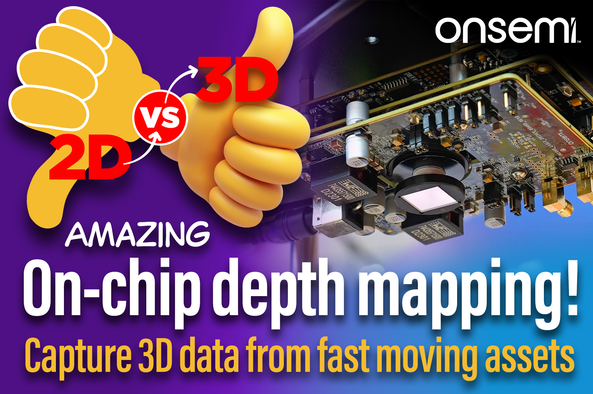
There are few things more satisfying at Embedded World than seeing a good old-fashioned train set being used to demonstrate bleeding-edge tech. But don’t be fooled by the nostalgic vibes—what onsemi is showing off here is seriously smart. This isn’t your average toy. It’s a real-world industrial application featuring cutting-edge depth mapping for machine vision, built right into a compact, low-power sensor solution.
Why Depth Mapping Matters
Most machine vision systems can handle 2D imaging with ease. That’s old hat. But when it comes to real-world asset tracking—whether it’s bottles on a conveyor, parcels in a warehouse, or oddly-shaped objects in logistics—depth information makes all the difference. Height, shape, and 3D profiling are essential for automation to function accurately, efficiently, and without hiccups.
That’s where onsemi’s indirect time-of-flight (iToF) solution steps in, solving the long-standing challenge of acquiring high-quality depth data—while objects are in motion.
In-Motion Insight: No More Stopping the Line
Many traditional iToF solutions require the conveyor to stop in order to get accurate depth readings. But onsemi’s tech doesn’t hit the brakes. Thanks to a smart iToF sensor with a global shutter, the system captures detailed depth maps in real-time, on the move—just like a high-speed industrial camera.
This matters for productivity. It also means no expensive stereo camera set-ups (and no complex post-processing pipelines) are needed. With onsemi’s sensor, it’s all processed on-chip, freeing up system resources and simplifying integration.
What Do You Actually Get?
onsemi isn’t selling you a finished camera—they’re providing the depth sensor at the heart of it all. What they do provide is a comprehensive reference platform, including:
- On-chip depth processing
- Monochrome imaging functionality
- Integration-ready reference modules
- Partnerships with camera makers like IDS Imaging for plug-and-play solutions
Whether you want to build your own custom camera, adapt a reference design, or just pick up a finished depth-mapping unit, onsemi gives you the flexibility to choose your path.
Evaluating the Technology
If you’re a design engineer looking to explore depth mapping for machine vision, onsemi offers multiple entry points:
- Evaluation kits for engineers who want to design their own systems
- Reference modules for faster prototyping
- Finished cameras from partners for instant deployment
Each option comes backed by robust ecosystem support—covering optics, laser guidance, and calibration advice—so you’re not building in the dark.
Whether you’re tracking assets in a smart factory, automating logistics, or scanning 3D surfaces, onsemi’s iToF solution brings depth and clarity to your vision—without ever needing to hit the brakes.
Comments are closed.
Comments
No comments yet