Products
Solutions
Published
19 January 2026
Written by Harry Forster
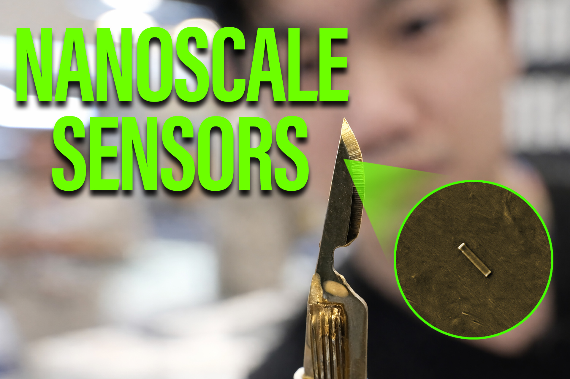
At CES 2026 in Las Vegas, digid demonstrated something that immediately challenges how design engineers think about sensor integration. Instead of asking where a sensor can fit, digid starts by asking where sensing is needed, then prints the sensor directly there. The result is a digid nanoscale sensor so small it often requires a microscope to see, yet robust enough for real industrial and medical use.
Most sensors today are already compact, but they are still discrete components that need board space, packaging, wiring, and mechanical accommodation. The digid nanoscale sensor approach removes that constraint entirely by allowing sensors to be printed at micrometre and even nanometre scale directly onto real objects, surfaces, and components.
Why nanoscale sensing matters
The value of a digid nanoscale sensor is not just its size, but what that size enables. In many designs, the most interesting data exists exactly where traditional sensors cannot go. This might be on a surgical tool, inside a thermal interface material, or on a structural element that experiences strain in operation.
By printing sensors directly onto these surfaces, engineers can measure temperature, force, strain, and pressure without redesigning the system around the sensor. In practice, this opens up new sensing points in medical devices, industrial equipment, electronics cooling, and mechanical assemblies.
Rather than compromising between performance and integration, a digid nanoscale sensor allows sensing to become part of the object itself.
From scalpels to processors
One of the most striking demonstrations at CES was a standard surgical scalpel fitted with printed strain sensors. Visually, it looked identical to a conventional scalpel, with no added bulk or mechanical change. Functionally, it became a smart surgical tool capable of measuring cutting forces in real time.
The digid nanoscale sensor was printed directly onto the metal blade after surface preparation and metallisation. Because the sensor is so thin and lightweight, it does not alter the feel or balance of the instrument. For surgeons, nothing changes. For engineers and researchers, entirely new data becomes available.
Another demonstration focused on thermal monitoring in processors. digid showed temperature sensors embedded directly inside the thermal interface material between a CPU die and its heat spreader. This allows temperature to be measured exactly where heat transfer occurs, rather than relying on indirect measurements elsewhere on the board. Using a digid nanoscale sensor in this way enables more accurate thermal profiling, better detection of hotspots, and improved control of throttling without consuming valuable silicon area.
Printed sensors, not packaged components
A key distinction with digid is that these sensors are not simply small components. They are printed structures that can be applied directly to metals, foils, ceramics, and other substrates. Depending on the application, a digid nanoscale sensor can be printed as a single sensing element or as part of more complex arrangements such as Wheatstone bridges for temperature compensation and multi axis strain measurement.
Because the sensing layer is so thin, it can be added to existing designs late in development without major mechanical or electrical changes. This makes the technology particularly attractive for retrofitting sensing into legacy systems or prototypes where redesign is not feasible.
Where engineers can use this today
The applications shown at CES only scratch the surface. A digid nanoscale sensor is well suited to medical tools, industrial condition monitoring, electronics thermal management, and structural health monitoring. Any application where size, weight, or placement has previously limited sensing is a candidate.
For design engineers, the key takeaway is that sensing no longer has to be constrained by component form factors. With printed nanoscale sensors, measurement can be placed exactly where the physics happens.
As systems become more compact and more data driven, technologies like the digid nanoscale sensor fundamentally change how and where engineers can observe the real world.
Comments are closed.
Comments
No comments yet