Products
Solutions
Published
19 May 2025
Written by Harry Forster
Evolution at Embedded World: Dream Chip’s 3rd-Gen SoC Steps Up
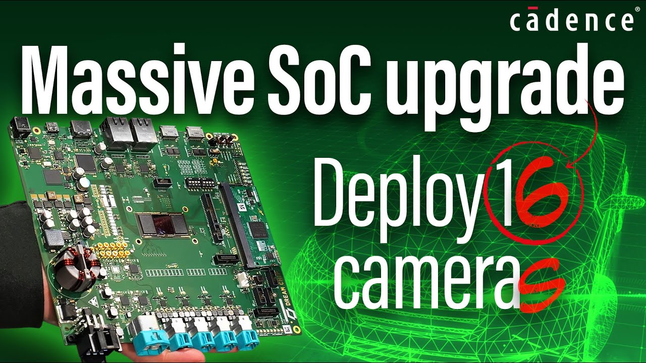
At Embedded World 2025, we met Dream Chip at the Cadence booth with a familiar setup—model cars and bold ambitions—but this year’s story is all about massive evolution. What once handled a single camera input and basic object detection is now a full-blown automotive vision and radar SoC powerhouse, integrating AI acceleration, radar fusion, and support for up to 16 cameras.
What’s New? More Cores, More Sensors, More Everything
Twelve months ago, their system-on-chip platform was focused on AI-based object detection using vision data. Today, Dream Chip has amped it up with 13 processor cores, three Cadence Tensilica Vision DSPs, 12 FFT accelerators for radar, and second-gen ISP improvements for real-time HDR image processing.
Need to connect 16 cameras with low-latency HDR? Done. Need radar and camera fusion in the same system? Absolutely. With high-bandwidth interfaces including PCIe and Gigabit Ethernet, this platform’s built to be the brain of next-gen automotive ECUs.
Vision Meets Radar: One Chip to Rule Them All
For developers tackling advanced ADAS applications, the ability to combine radar data with high-res camera feeds—on one SoC—is no small thing. The board’s new GMSL interface allows simultaneous connection of multiple sensors, perfect for surround-view systems or sensor fusion pipelines.
And it’s not just about connectivity. Thanks to low-latency ISP and tightly optimised real-time processing, the system handles tunnel exits, glare, and dynamic driving environments like a pro—turning mobile-style HDR into automotive-grade performance.
Built for the Future: AI-Ready, Latency-Low, DSP-Offloaded
Dream Chip didn’t just add power—they added practicality. The architecture offloads AI workloads intelligently, freeing up ARM cores while handling edge-case operators on DSPs. As AI frameworks evolve faster than hardware can keep up, this flexibility is a serious win for developers aiming to future-proof their designs.
Built on GlobalFoundries’ 22FDX node, the new SoC more than doubles the silicon real estate of its predecessor—from 92 mm² to 217 mm²—all with a focus on real-world deployment and customer flexibility.
Comments are closed.
Comments
No comments yet