Holtek’s HT32 MCUs are based around a next-generation ARM Cortex-M3 processor core that is tightly coupled with a Nested Vectored Interrupt Controller (NVIC), SysTick timer, and includes advanced debug support. With flexible package options – 46-pin QFN or 48/64/100-pin LQFP – and an operation temperature range of -40°C to 85°C, these MCUs are suitable for a wide variety of applications and circuit topologies.
Holtek’s HT32 MCUs operate at a frequency of up to 96 MHz with a Flash accelerator to obtain maximum efficiency, and they provide up to 256 kB of embedded Flash memory for code/data storage and 128 kB of embedded SRAM memory for system operation and application program usage. A variety of peripherals, such as ADC, I2C, USART, UART, SPI, I2S, PDMA, GPTM, MCTM, SCI, EBI, CRC-16/32, AES-128/256, USB2.0 FS, SDIO, CSIF (HT32F22366 model only) and SWJ-DP (Serial Wire and JTAG Debug Port) are also implemented in the devices’ series. Additionally, several power-saving modes provide flexibility for maximum optimisation between wakeup latency and power consumption. Real-Time-Clock (RTC) functionality with an alarm function allows for interrupt and wake-up events.
The on-chip ADCs offer a 12-bit SAR engine with up to 1 Msps conversion rate. Up to 16 external analogue input channels can be connected to the device, though multiplexing means that only 2 internal channels can be measured simultaneously. The ADC can be operated in one shot, continuous, and discontinuous conversion modes.
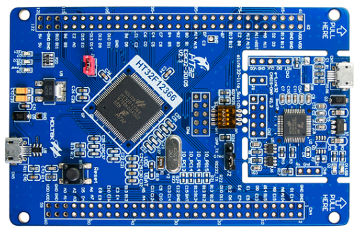
The ESK32-30105 development board and software development platform is designed to help new users start using this device in the shortest possible time frame. For the most flexibility, the ESK32-30105 uses the 100LQFP package version of the HT32F12366 and comprises of a target board and serial-wire debugger. When operating the device, one can use the target-board external power supply or power the device by the e-Link32 Pro USB supply.
(All images sourced from Holtek)

