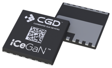
Featuring their ICeGaN™ technology, the CGD65A055S2 from Cambridge GaN Devices is an enhancement mode GaN-on-silicon power transistor, exploiting the unique material properties of GaN to deliver high current, high breakdown voltage, and high switching frequency. The device comes in a DFN 8×8 SMD package with a built-in clamping structure to support high-frequency operation while ensuring the highest thermal performance. With uncompromised GaN switching performance or RDS(on), without the need for negative gate voltages to turn off – ON-state threshold at around 3 V – the CGD65A055S2 can be operated with virtually all gate drivers and controller chips available.
The CGD65A055S2 is rated at 650 V at 55 mOhm with a maximum DC current of 27 A and a peak gate voltage of 20 V. The integrated current sense function eliminates the need for a separate current sense resistor and the associated efficiency losses, and because no external sense resistor is needed, the device can be directly soldered to the large copper area of the ground plane, simplifying thermal design and enabling the device to run at around 20°C cooler than a silicon equivalent device. ICeGaN also extends the gate window and allows the CGD65A055S2 to be driven like a MOSFET.
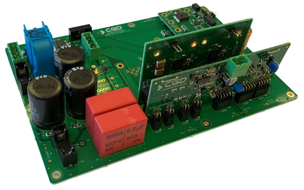
The 350 W Half Bridge LLC Evaluation Board (CGD-UG2204) uses a modular, high-efficiency LLC Topology, allowing users to easily realise the performance benefits of ICeGaN and easily change differing circuit elements to tune circuit performance. Specified at 330-420 VDC Input, 20 VDC Output, the evaluation board uses two CGD65A055S2 devices, an ICeGaN Gate with 9-20 V drive, a UCC256402 LLC controller, an SRK2001 synchronous rectifier controller on output with two 80 V MOSFETs, and an example resonant tank design (series inductor + transformer + resonant capacitor) for a maximum efficiency of 96.3%. The circuit components that can be swapped are the controller board, GaN switch board, synchronous rectifiers board, resonating inductor, and the transformer, and the minimum required equipment to operate this board is a high-voltage DC supply, optional low-voltage DC Supply, and a suitable load.
(All images sourced from Cambridge GaN Devices)


