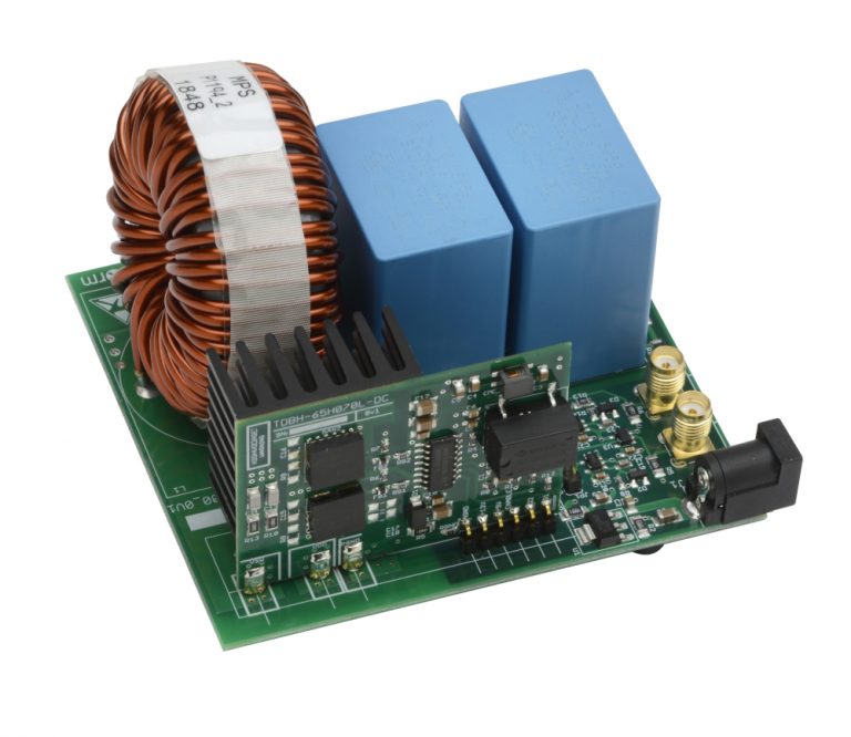
Transphorm’s 1.2 kW half-bridge synchronous buck or boost evaluation platform provides designers with an easy-to-use configuration to test the switching characteristics and efficiency of Transphorm’s GaN FETs. This evaluation board features a variable switching frequency from 50 kHz to 300 kHz and can operate with up to 400 VDC input or output in the buck or boost modes.
This platform uses Transphorm’s TP65H070L 650 V GaN FETs, which are available in an 8 x 8 mm PQFN package with the engineer’s choice of the drain or the source connected to the largest of the 3 pads. These devices are an innovative fusion of state-of-the-art GaN HEMT technology and low-voltage silicon MOSFET technology, which creates a GaN solution with superior reliability over competitor alternatives. The main benefits of Transphorm’s GaN is improved efficiency over silicon due to the reduced gate charge, crossover loss, and reverse recovery charge. This is illustrated in the key specifications of the device:
-> VDSS: 650 V
-> VDSS(TR): 800 V
-> RDS(On)eff max.: 85 mΩ
-> QRR typ.: 89 nC
-> QG typ.: 9.3 nC
Transphorm’s solution can be driven using commonly used gate drivers and allows for increased power density, reduced system size and weight, and lower overall system cost in applications including data communications, industrial devices, PV inverters, and servo motor controllers.
The full datasheet for the TP65H070L device can be found here, and a user guide for the evaluation platform can be found here.
If you’ve got a commercial project where you would like to evaluate Transphorm’s GaN, fill out the form below, and ipXchange will put you in touch to discuss your project and the best evaluation platform for your requirements.


