Cologne Chip’s GateMate series of FPGAs feature best-in-class logic capacity, power consumption, package size, and PCB compatibility while being among the lowest-cost FPGAs in the industry. This enables designers to use small- to medium-sized FPGAs in projects that would have previously been unviable, whether that be for a university project or a high-volume commercial application. Additionally, these devices are the first FPGAs to be made in Europe, and an easy supply chain, with manufacturing using GlobalFoundries in Dresden, ensures supply and the shortest lead times.
The GateMate FPGAs are based on a novel architecture that combines programmable elements (CPEs) with a smart routing engine, which allows for efficient building of arbitrarily sized multipliers. Memory-aware applications can use block RAMs with bit widths of 1 to 80 bits, and GPIOs can use different voltage levels from 1.2 to 2.5 V. These can be configured as single-ended or as differential pairs to suit your application, with support for double data rate (DDR).
A key benefit of Cologne chip’s FPGAs is their low power consumption and lack of excessive start-up currents. 3 operation modes – low power, economy, and speed – further support low power consumption. The two-supply-rail architecture, where either rail can be switched on first, makes FPGA implantation with GateMate devices simple for new users of the technology.
FPGA designs are synthesised using the open-source Yosys framework, and the free Cologne Chip P&R-software can be used to generate the FPGA bitstream. A Static Timing Analysis (STA) can also be performed to provide evidence about critical paths and the overall performance of a design.
The CCGM1A1 is the smallest of the GateMate devices and is ideal for low-power applications. The 20,480 CPEs correspond to 20,480 8-Input-LUT trees or 40,960 4-Input-LUT trees with 40,960 flip-flops/latches. Each CPE is configurable as a 2-bit full-adder or a 2×2-bit multiplier. This device is supported by 1280 kb block RAM in 64x 20 kb blocks or 32x 40 kb blocks, with 4x PLLs, 1x SerDes at 5 Gb/s, and 162 single-ended I/Os.
The chip supports fast configuration with a quad SPI interface running at up to 100 MHz, as well as multi-chip configuration with multiple clocking schemas. Other models of GateMate FPGA are available, soon to be with up to 512,000 programmable elements, but the CCGM1A1, CCGM1A2, and CCGM1A4 devices – with 1, 2, and 4 times the relative number of programmable elements, supporting memory, PLLs, and SerDers – are PCB footprint compatible and use a 324-ball BGA package (15 x 15 mm). This means that no redesign is required when switching between these first three devices of the family, and only 2 signal layers are required on the PCB, further simplifying implementation of FPGAs.
More information on the full range of GateMate devices can be found in this datasheet.
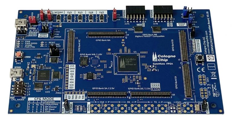
Cologne Chip makes an evaluation board that can be used as a development platform or reference design when getting started with the CCGM1A1 GateMate FPGA. 2 Pmod-compatible ports enable easy integration of many peripheral boards across a wide variety of applications, and the 6 GPIO banks can be used to further support your design journey.
The board also features 64 Mb Quad-I/O SPI flash @ 80 MHz and 64 Mb HyperRAM @ 166 MHz with an unpopulated footprint for adding a secondary HyperRAM or HyperFlash module. The SerDes interface is provided via SMA connector, and 2 USB ports are present for JTAG/SPI configuration and powering the board. For those who are interested, more information on this evaluation platform can be found in this datasheet.
If you are looking to get started using FPGAs in your commercial application, consider Cologne Chip’s solution by filling in the application form below, and ipXchange will put you in touch with Cologne Chip to facilitate evaluation of their technology.


