Now that’s a lot of lows, but all Flo Rida references aside, Gowin’s LittleBee® product family provides a compact solution for those looking for flash-based, non-volatile FPGAs with an abundance of logic resources, multiple I/O standards, embedded RAM, DSPs, PLLs, embedded security, and additional user flash.
Though Gowin states that their LittleBee FPGAs are leading the industry in I/O intensive source synchronous interfacing and bridging applications such as MIPI CSI-2, MIPI DSI, USB 2.0, Ethernet, HDMI, MIPI I3C and more, they also offer security, automotive, and Bluetooth LE specific configurations, as well as an ultra-low-power model. LittleBee FPGAs are also an ideal candidate for hardware management applications, and the family is complimented by multiple innovative product line sub-features such as extended memory and hardened ARM Cortex-M processor cores, which expand the capabilities and usage compared to traditional FPGA products. Any additional features understandably result in a package size increase – the minimum size is 2.3 mm x 2.4 mm (CS30) growing to 20 mm x 20 mm (eg. LQ144) for the largest in the family – but even in the smallest, most basic package, there is the capability for 120 I/Os with 96 Kb flash and 72 Kb block SRAM.
Gowin also provides highly optimized and easy-to-use FPGA development software to support the LittleBee product family, which includes synthesis, mapping, placement, routing and bitstream generation, along with programming tools, an embedded logic analyser, and a power calculator. Multi-boot and support for JTAG, MSPI, SSPI, I2C, and CPU standards make for an extremely flexible programming interface.
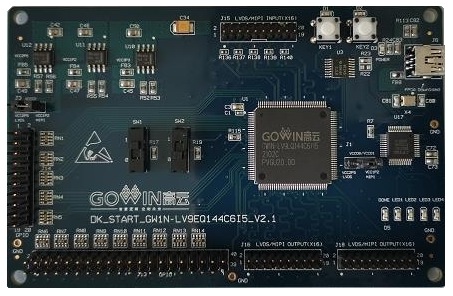
Gowin makes several development boards for the LittleBee family, but for the purpose of this article, I will discuss that which uses the GW1N-9 FPGA, the largest spec model of the traditional (non-expanded) LittleBee FPGAs. This model includes additional shadow SRAM at 17,280 bits of capacity, 468 Kb block SRAM, 608 Kb flash, and a maximum of 276 I/Os. As with others in the range, the GW1N-9 has the same characteristics of low power consumption, instant-start, low cost, non-volatility, high security, convenient and flexible usage, etc., which can effectively reduce the learning cost and help users to quickly integrate such devices. This development board offers abundant external interfaces, including MIPI/LVDS interfaces, GPIO interfaces, etc. There are also sliding switches, button switches, and other resources for developers to use.
Keep designing!
(Image sourced from Gowin)
You must be signed in to post a comment.
Comments
No comments yet